Research & In-house PCB Prototyping

Multilayer Solutions

Multilayer Circuit Boards

Production of up to eight layers in-house

LPKF offers a complete prototyping product line for production of multilayers in an in-house lab. The multilayers are produced in three simple steps: structuring, lamination, and through-hole plating.

A Printed Circuit Board Composed of Several Layers

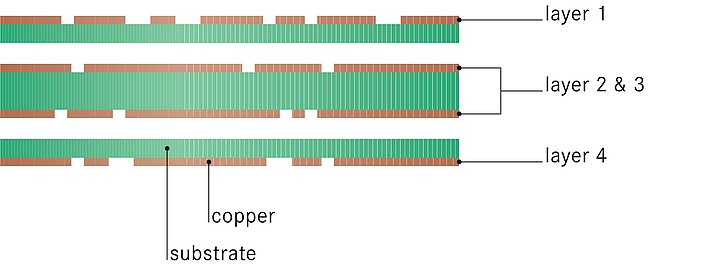
A multilayer is made up of multiple layers that are laminated together to form a printed circuit board. The outer layers of a multilayer are usually single-sided PCBs, whereas the inner layers are double-sided materials. Insulating layers, so-called prepregs, are inserted between the conductive layers. Up to four layers can be through-hole plated in a chemical-free process. For electrical connection of up to eight layers through-hole electroplating is recommended.

Three Steps to a Multilayer

Structuring of traces
Structuring

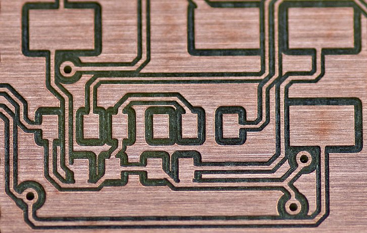
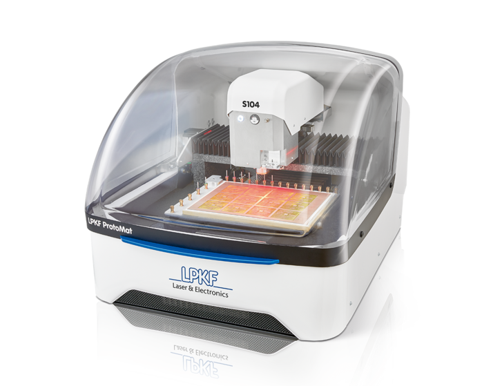
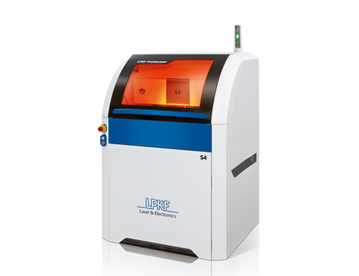
An LPKF ProtoMat circuit board plotter or an LPKF ProtoLaser structures the traces on the base material using the layout data. Supported by automatic tool change and a camera for recording of fiducials, the system accomplishes this layer by layer – nearly automatically.

Pressing of structured PCB layers
Lamination

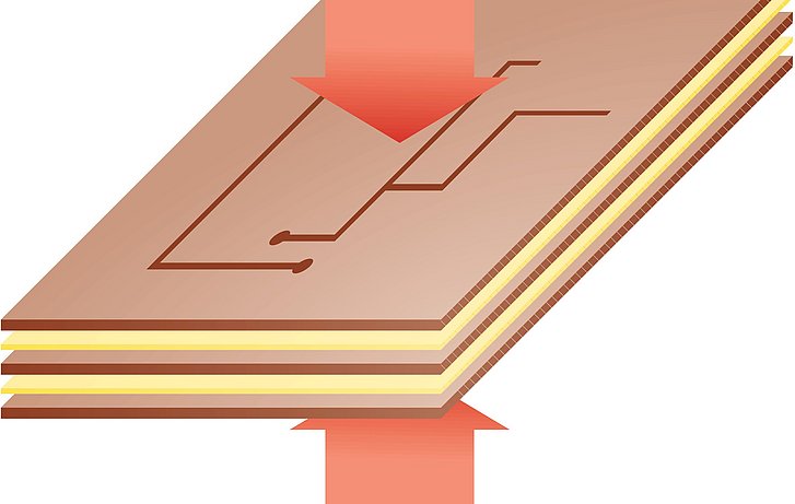
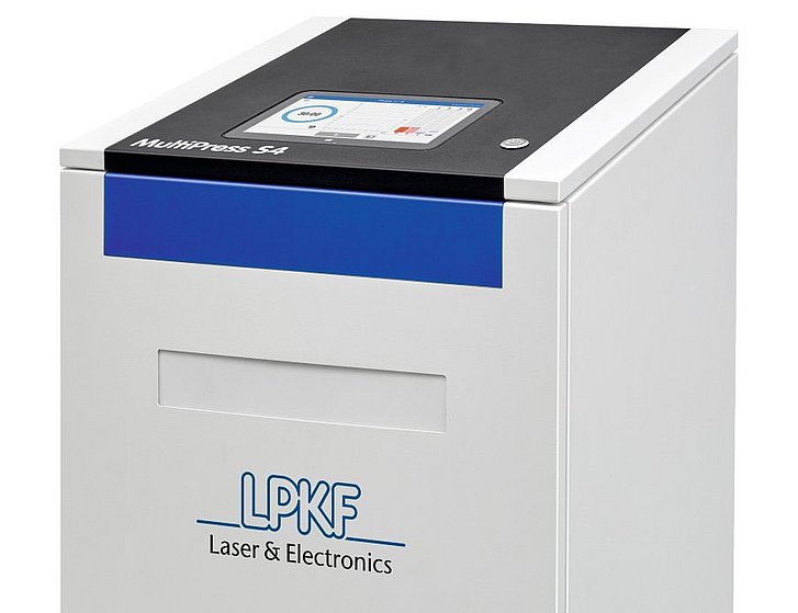
The structured layers are precisely stacked. Between the layers, “prepregs” insulate the traces on the different layers. During lamination the prepregs connect the layers. The LPKF MultiPress S hydraulic press performs the task of lamination– with perfect results, even for HF multilayers, thanks to preset process profiles.

Through-hole plating of the multilayer printed circuit board
Through-hole plating

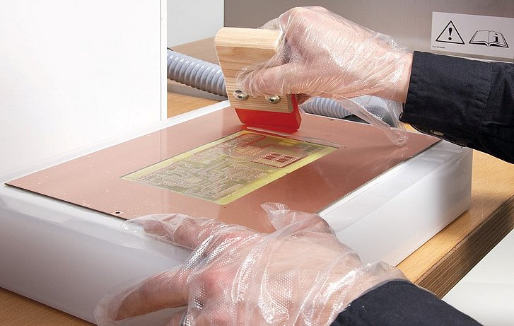
The electrical connections between the individual layers form the final conductor structure. The LPKF ProtoMat circuit board plotter drills the through-holes. LPKF ProConduct is used for electrical connection – in a chemical-free process using a special conductive paste. For more than four layers, through-hole electroplating is recommended.

Video Inhouse PCB Multilayer Process

Systems for Multilayer Production

Structuring
Lamination
Through-hole plating
Circuit board plotter LPKF ProtoMat S104

The circuit board plotter specialist for RF and microwave applications.

Structuring laser system LPKF ProtoLaser S4

With the LPKF ProtoLaser S4, a structured printed circuit board can be produced from the layout within a few minutes – with exact geometries on numerous substrates.The ProtoLaser S4 can also reliably process copper areas with inhomogeneities of up to 6 µm in size and is ideal for manufacturing multilayers.

The LPKF MultiPress S4 features a short pressing time of approx. 90 minutes and sophisticated temperature management. Storable pressure and temperature profiles provide optimum support for the user.

[Translate to USA:] LPKF ProConduct

The electrical connections between the individual layers are made by LPKF ProConduct, a chemical-free system specially developed for laboratory use. If there are more than four layers, galvanic through-hole plating is recommended.

[Translate to USA:] LPKF Contac S4

With multilayers, the connection of layers with vias is of particular importance. The classical galvanic process is obligatory for six layers or more. The LPKF Contac S4 table system is easy and safe to operate without chemical knowledge.

 Downloads

Brochure
8-Layer Multilayer in Your Own Lab – LPKF MultiPress S4 (pdf - 271 KB)
Download
Brochure
LPKF MultiPress S4 (pdf - 146 KB)
Download
Brochure
LPKF Multilayer Technology for the Laboratory (pdf - 459 KB)
Download
Prototyping Catalog
Rapid PCB Prototyping Product Catalog (pdf - 4 MB)
Download
Prototyping TechGuide
LPKF TechGuide Rapid PCB Prototyping (pdf - 3 MB)
Download

 Contact Us

Logo:   LPKF Laser & Elektronics